MZ Technologies’ GENIO Tool Suite adopted for Major System-in-Package IC
An internationally respected System/ASIC company is adopting MZ Technologies’ GENIOTM 1.7 fully-integrated EDA co-design tool.
The company adopted a full-suite license and has targeted a next generation global semiconductor product family based on heterogeneous advanced technology system-in-package (SIP.) Details of the design remain scant due to the propriety nature of the underlying technology.
The licensing agreement marks a major milestone for MZ Technologies, representing its initial entry into the broad Asian market.
“To be the co-design tool of choice in the international marketplace is a huge step forward,” said Anna Fontanelli, Founder and CEO of MZ Technologies. “It is global confirmation of the tool’s contribution to the future of chiplet-based and advanced hybrid package design.
GENIOTM 1.7 is the first commercial integrated silicon/packaging co-design tool, available to IC and IC Package design leading companies. Its cross-hierarchical, 3D-aware, design methodologies streamline the entire IC eco-system. It integrates IC and advanced packaging design to ensure full system level optimization, shorten the design cycle, drive faster time-to-manufacturing and improve yields.
GENIOTM 1.7 co-plans the final packaged device and integrated electronic circuits (ICs) in complex 2.5-3D chiplet-based hybrid configurations and was recognized by an international jury of industry experts as a revolutionary EDA co-design tool.

The GENIOTM tool also easily integrates existing silicon and package EDA flows to create full co-design and optimization of complex multi-chip designs that comprise advanced heterogeneous microelectronic systems.
GENIOTM 1.7 licensed under this agreement features Parasitic Estimation and Stack Planning functionality that slash total design time and reduces overall design complexity.
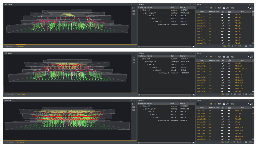
Parasitic Estimation enables early-on system analysis, based on virtual routes, prior to physical implementation. Stack Planning Support automatically identifies the best 3D stack configuration, given physical and electrical constraints. It provides a more efficient chiplet-based 3D-IC system organization and electrical performance, while reducing the physical resources (TSVs) required for vertical interconnect.


